Nordson details how bond testing is shifting from sampling to data-driven process control in advanced packaging
Nordson's Semiconductor Engineering analysis shows bond testing moving beyond spot-checks toward AI-driven, wafer-mapped sampling as interconnect dimensions shrink to a few microns.
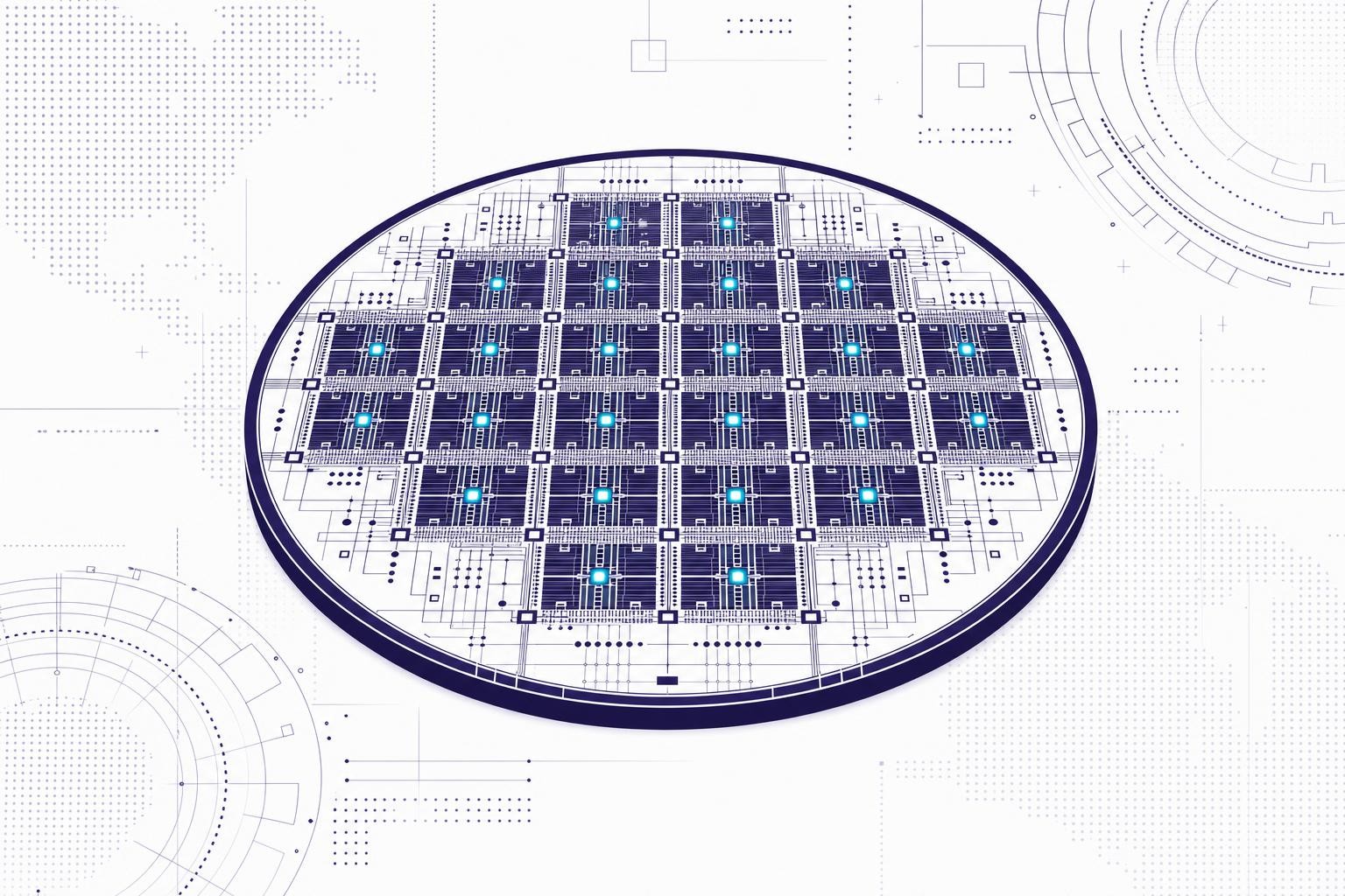
A Semiconductor Engineering analysis published 19 August 2026 by Nordson's test and inspection division sets out why wafer-level bond testing is being repositioned from a quality gate into a continuous process-control tool, as interconnect dimensions shrink to just a few microns and advanced packaging formats multiply the ways those connections can fail[1].
Why bond integrity is the new yield limiter
Interconnect dimensions in leading-edge devices are now measured in just a few microns, with thousands - and in advanced devices, millions - of bumps distributed across a single wafer[1]. At that scale, small variations in materials, deposition, or process conditions can produce inconsistencies in bond formation that are invisible to optical inspection but still capable of causing field failures[1].
The stakes are rising because semiconductors are moving deeper into high-reliability end markets. A weak bond that might cause a dropped call in a smartphone can translate into a safety event or a costly recall in an automotive or aerospace system[1]. Increasing scrutiny around product longevity and electronic waste is adding a second pressure: durability must be engineered in from the start, not screened for at the end of the line[1].
Where advanced packaging makes measurement harder
Fan-out wafer-level packaging (FOWLP) is a particular pressure point.
The challenges that make measurement difficult include:
- Warpage in FOWLP substrates, which shifts the test surface out of the calibrated measurement plane
- Uneven stress distribution in 3D stacked structures, producing bond-strength gradients across the wafer
- Material complexity, as new dielectrics and metal systems interact differently under applied force than conventional solder bumps
- Scale, where millions of interconnects per wafer make static, manually defined sampling plans statistically inadequate
From static sampling to dynamic, context-aware testing
Historical static or manually defined sampling strategies now struggle to keep pace with the complexity of modern advanced packaging[1]. Nordson's response, described in the Semiconductor Engineering piece, is wafer mapping and matrix-based selection built into its BT4800 INTEGRA Plus system, which allows engineers to target specific die, regions, or known areas of risk rather than pulling fixed-position samples[1].
The system pairs mechanical bond-strength data with Nordson Intelligence, an AI-powered failure-mode grading layer that links force measurements to failure details and wafer-level context[1]. The goal is faster root-cause identification and tighter feedback into process parameter adjustment - a loop that manual approaches cannot close at the throughput modern fabs require[1].
Automated, software-driven bond test platforms are becoming central to modern semiconductor manufacturing as the focus shifts from individual measurements to how those measurements are generated, interpreted, and applied at scale[1].
The next test for this approach will be whether dynamic sampling strategies can be validated against automotive-grade qualification standards - AEC-Q100 and its successors - where the statistical confidence requirements are among the most demanding in the industry. As chiplet-based designs push more heterogeneous interfaces into safety-critical applications, that validation work is likely to define the next phase of bond-test platform development.
Written by Electronics Insider's automated desk from the sources above and published automatically. How we work.
Related
 Semiconductors
Token spend is becoming a line item in EDA project budgets, DAC roundtable finds
A closed-door DAC 2026 roundtable with Cadence, Synopsys, Siemens EDA, Keysight, and ChipAgents found token cost has moved from an afterthought to a formal budget concern in chip design projects.
10 Sept 2026 Design & EDA
Cadence's Amol Borkar explains why AI voice at the edge demands a rethink of SoC architecture, not just faster processors
Semiconductor Engineering's interview with Cadence's Tensilica DSP lead lays out why NLP is reshaping audio SoC design - and why raw clock speed is the wrong lever to pull.
10 Sept 2026 Design & EDA
French gendarmerie researchers show voltage glitching bypasses eMMC password locks on 3 of 10 commercial parts, with measurable evidence alteration
A paper from France's Institut de Recherche Criminelle quantifies both the success rate and the data-integrity cost of fault-assisted eMMC access in forensic investigations.
10 Sept 2026